


More from Jerry Proctor


More in Politics

Related Blogs
Les archives
Partage Social
10 Things You Might Not Know About Wafer Dicing
Posté par Jerry Proctor
Corps
In this blog article, you will learn some interesting facts about wafer dicing. Take a look at the 10 things you might not know about wafer dicing!
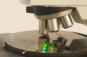
What is Wafer Dicing?
Wafer dicing is a process used to create small, individualized pieces of semiconductor materials. This process is used in many different industries, including electronics, communication, and medical devices.
Wafer dicing typically involves cutting thin slices of a semiconductor material. These slices are then separated by using a sharp blade or other tool. This process allows for the creation of small, individualized pieces of the material.
One important advantage of wafer dicing is that it allows for the creation of customized products. This means that companies can create products that are specifically designed for their needs. Wafer dicing also allows for the production of large quantities of product quickly and without any waste.
Why Wafer Dicing is Important
One of the most important tasks that engineers and scientists perform is wafer-level fabrication. This is the process of cutting and designing small electronic circuits and devices using tiny, precise cuts.
Wafer-level fabrication is crucial for a number of reasons. First, it allows for the creation of more complex and powerful devices. Second, it enables the manufacture of products in smaller sizes. And finally, it allows for faster and more accurate production times.
In addition to its importance in electronics manufacturing, wafer-level fabrication is also used in other industries, such as healthcare and automotive manufacturing. It has even been used to create prosthetic body parts.
Given all of its benefits, it's no wonder that wafer-level fabrication is one of the most in-demand skillsets in today's market. If you're interested in pursuing a career in engineering or science, be sure to consider wafer-level fabrication as an option.
How Wafer Dicing is Done
1. Wafer dicing is a process used to create small pieces of semiconductor material.
2. Wafer dicing is done using a variety of techniques, including laser cutting and etching.
3. The small pieces of semiconductor material created by wafer dicing can be used in a variety of applications, including consumer devices and computers.
Types of Circuits
Wafer dicing is a process of cutting thin pieces of semiconductors from larger chips. There are many different types of circuits that can be created using wafer dicing, and each has its own unique advantages.
One type of circuit that is often used in electronics is the field-effect transistor (FET). FETs are small devices that are made from two semiconductors layers that are placed one on top of the other. When voltage is applied to the two layers, they become insulated from each other, allowing current to flow between them. This type of circuit is used in digital devices, such as digital cameras and smartphones.
Another type of circuit that is often used in electronics is the bipolar transistor (BJT). BJTs are similar to FETs, but they have an extra layer between the two semiconductors. This layer allows current to flow in only one direction, which makes BJTs more efficient than FETs. BJTs are also used in digital devices, but they are usually less efficient than FETs.
However, BJTs have one major advantage over FETs: they can be turned off completely. This means that they can be used as switches,
Results and Conclusion
1. Wafer dicing is a process that is used to create small pieces of a given material.
2. Wafer dicing can be used to create a variety of different products, including semiconductors and LED chips.
3. The results of wafer dicing are very dependable and accurate.
4. Wafer dicing is a very common process, and it is used in many different industries.


commentaires