


More from Amelia Smith


More in Politics

Related Blogs


Les archives
Partage Social
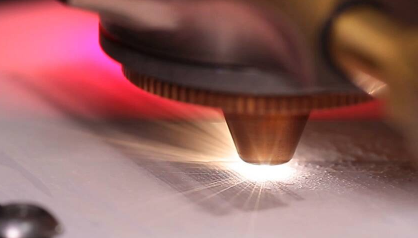
Downsizing Wafer Laser
Corps
Downsizing wafers is a method of laser cutting a wafer to a specified diameter. The process involves entering coordinates into a computer and the laser cuts the wafer accordingly. Multiple holes can be cut out of the wafer or the entire wafer can be downsized. If required, the wafer can be re-cut at a later date. Diameter tolerances of 0.05mm are possible. read out for more about downsizing wafer laser;
LatticeGear's LatticeAx
The LatticeAx downsizing wand laser is a versatile tool that cleaves crystalline materials with a 500-micron diamond tip. The downsized sample is then guided on the front side of the wafer using a sample holder. This laser cleaves a single crystal in a wafer-scale manner, while the operator works on the reverse side. The process is site-specific, and the cleaving is done with little force. It can also cleave samples smaller than a wafer-scale substrate.
The LatticeAx is an effective wafer-cleaving solution. It has a low-cost, high-throughput option. It is a great solution for laboratories that need to cleave a large number of samples. In addition to cleaving, it can also be used to improve cross-section sample quality and preparation.
The LatticeAx is a stand-alone tool that requires a flat, stable surface. It does require a power source, but the machine is mobile and can cleave a full wafer. It is also easy to use and requires only a small footprint. If you are looking for a downsizing wafer laser that is a great value, the LatticeAx downsizing wafer laser is the tool for you.
LatticeGear's Flipscribe
The new downsizing wafer laser from LatticeGear is perfect for cutting sapphire and other difficult-to-cleave materials. This machine features mechanical platforms and methods that combine diamond indenting, scribing, and cleaving. These tools are repeatable and allow for new test conditions. These features make the Flipscribe a valuable addition to any lab.
The company launched its own downsizing wafer laser in 2012 and has since become an industry leader. The company's products have helped many companies increase productivity by up to 50 percent. The company offers kits to meet specific application requirements. The company's products are designed to deliver quick turnarounds and high-quality results. Flipscribe, LatticeAx, and LatticeGear are registered trademarks of LatticeGear.
The Flip Scribe downsizing wafer laser uses new techniques to cleave III-V substrates. This allows users to scribe the back-side of a wafer without touching the surface. This eliminates the chance of contamination of sensitive front-side devices. The laser's compact design allows for quick and clean downsizing. The Flipscribe downsizing wafer laser is fast, accurate, and has an affordable price tag.
Synova laser microjet
With its proprietary Laser MicroJet technology, Synova offers a cost-effective alternative to diamond saw cutting and conventional laser machining. These systems can produce high-volume manufacturing of semiconductors, thin films, and devices. By using a high-pressure water jet and a high-power laser beam, Synova's proprietary system cuts complex materials and shapes quickly and reliably. To learn more about Synova's Laser MicroJet, click here.
The Synova Laser MicroJet is a new type of downsizing wafer laser based on water jet guided laser cutting. The new technology enables outstanding results for cutting, drilling, scribing, edge grinding, and thinning. This machine comes with a quick quality check and is suitable for use in the semiconductor industry. In addition, it also has an integrated vacuum for collecting particles and dust as the laser travels through the wafer.
This technology can downsize wafers up to 450mm in diameter. It is ideal for cutting LED chips, which are made of difficult materials. The system is flexible enough to accommodate multiple materials and can be used on patterned and thick wafers. The system's high-power stream allows for multiple applications, including laser edge isolation and multi-directional 2D-cutting. The system can process up to 2,000 wafers per hour. During the process, it is possible to add a wafer orientation notch and milling. The technology is also suited for other applications, including downsizing wafers and semiconductor reactor parts.


commentaires